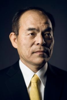
Shuji Nakamura
Biographical
Shuji Nakamura was born on May 22, 1954 in Oku, a tiny fishing village on the Pacific coast of Shikoku, the smallest of Japan’s four main islands. Farming is the principle occupation in Oku. Local farmers grow yams on steps cut into steep hillsides. Shuji’s maternal grandparents owned such a farm. To get to the nearest town, the villagers relied on a ferry. Inconvenient perhaps, but the village was an idyllic place to grow up.
Shuji’s father, Tomokichi, worked as a maintenance man for Shikoku Electric Power. From him, Shuji learned how to make wooden toys, like catapults and bamboo propellers. He liked making things and became good at it, a skill that would stand him in good stead.
At school Shuji was not academically gifted. His boyhood was typical. He fought constantly with his elder brother. Smaller than his sibling, Shuji always lost. Though physically defeated, mentally he would never give in. His mother was forever chiding her boys to do their homework. But for the most part, they ignored her admonishments.
Throughout primary and high school, Shuji’s passion was volleyball. There was no gym at the school, so his team had to practice outside in the mud. They tried hard, but rarely won. Fiercely competitive from an early age, Shuji always hated to lose. Volleyball left Shuji little time to study for his high school entrance exams. He was bad at rote learning, but good at math and science. Somehow, he managed to scrape into an academically-oriented school.
Here, too, volleyball remained his priority. His classroom teacher told him that to improve his scores, he would have to quit playing. It was time to concentrate on studying for the all-important university entrance exams. But he could not let down his team. Shuji was the only student in the A-stream to continue playing sports until graduation.
Shuji paid a price for his dedication to volleyball. His university entrance exam results were not good enough to win him a place at a prestigious school. Shuji’s dream was to become a theoretical physicist or a mathematician. But his teacher told him that he could not make a living from physics – he had better choose a course like engineering so that he could find a job.
Shuji picked electrical engineering because it seemed close to physics. In 1973, aged 19, he entered Tokushima University, a local state school. Many professors there were former high-school teachers. The textbooks were out of date.
His first two years consisted of general studies, including arts courses, which Shuji hated. He couldn’t understand why he had to take such irrelevant subjects. Soon he stopped attending classes. All day long he would read books, mostly on physics. But there was a limit to the amount he could absorb by reading alone. Finally, in his third year at Tokushima, Shuji attended a lecture on semiconductors. Fascinated by the physics of solid-state materials, he decided to stay on at university for a further two years and do a master’s degree under Professor Osamu Tada.
As his thesis topic, Shuji chose the conductivity mechanism of barium titanium oxide. His focus was theoretical. But Professor Tada was a dyed-in-the-wool experimentalist. He would catch his student reading papers and tell him that knowing theory was no use if he couldn’t make actual devices.
Tada’s lab was known as “the junk room.” It was crammed with broken televisions and old radios which could be cannibalized for spare parts. To build what they needed, students had to acquire manual skills – soldering, cutting and joining glass, beating and welding sheet metal, fashioning parts on a lathe.
Shuji remembered his days as a master’s student as like being a sheet-metal worker in a small factory. What he wanted was to study theory. But most of his time was taken up jury-rigging equipment for experiments. In fact, Shuji was gaining precisely the kind of skills that he would later need in his quest to develop a bright blue LED. As a corporate researcher, he would be forced to make or modify much of his own equipment. Ultimately it would largely be this technical mastery that would give him the edge on his rivals.
As a 25-year-old graduate student with a master’s degree in electrical engineering, Shuji expected one of Japan’s consumer appliance manufacturers would hire him. But the likes of Sony tend not to recruit graduates from local universities.
In his interview at Matsushita, Shuji made the mistake of discussing the theoretical aspects of his thesis research. We don’t need theoreticians, the firm’s recruiters told him. At Kyocera, he did better, emphasizing the practical applications of his work. The company offered him a job. But as the day on which Shuji was due to report for work in Kyoto neared, he had second thoughts. Prior to his job-hunting trips, he had rarely left Shikoku.
At the same time, he really wanted to work in a proper research laboratory at a major company. Torn between two paths, Shuji asked Professor Tada what he should do. Tada pointed out that in Tokushima, there were no jobs for electrical engineers. If Shuji elected to stay on the island, he would have to give up a career in his chosen field. Eventually Shuji decided to remain in Tokushima.
His professor introduced Shuji to Nobuo Ogawa, the founder-president of an obscure local chemical firm called Nichia. The company was initially reluctant to hire him, but Shuji refused to take no for an answer.
When Shuji joined in April 1979, Nichia had fewer than 200 employees. The firm made phosphors for color televisions and fluorescent lamps. These were mature markets. If Nichia was to grow, it needed new products.
Shuji was assigned to the company’s two-man development section. His first job was to refine high-purity gallium metal. This turned out to be a dead end. The company ordered him to produce gallium phosphide, a material used to make red and green LEDs. Knowing next to nothing about LED materials, Shuji had to start from scratch.
There was no budget for equipment. He had to scavenge, fixing broken parts by hand. To build his reactor, Shuji scrounged heat-proof bricks, cables, a vacuum pump, and an old electric furnace. He had to order quartz tubes. To seal the open-ended tubes so they could be evacuated, he had to learn how to weld quartz.
To make gallium phosphide you heat phosphorus in a tube. If the tube gets too hot, the phosphorus vapor expands, causing the quartz to crack. This lets in oxygen, which reacts with the phosphorus causing an explosion. Such explosions became a feature of Shuji’s time at Nichia. His lab would fill with white smoke. Ignited phosphorus would fly everywhere, along with shards of broken quartz. Shuji would run around pouring water over the burning phosphorus, desperately trying to douse the flames.
The blasts happened several times a month, often in the evening. The shock wave would hit his fellow-workers as they were heading for their cars in the parking lot. The first few times it happened, they dashed into his lab to see if he was alright. By the fifth or sixth time, however, they had become so used to the bangs they no longer came to check.
Eventually, Shuji succeeded in developing commercial-grade gallium phosphide. More satisfying than producing the material was how he felt when the company’s salesmen told him they had made a sale. It gave him pleasure to think that he had finally managed to contribute to the company’s bottom line. But only a little: the market for gallium phosphide was already crowded. A late entrant, Nichia was only able to win a sliver of the pie.
Shuji’s next assignment was to produce gallium arsenide, which is also used to make LEDs, typically infrared ones such as those found in television remote controls. But GaAs also has other applications, like the semiconductor lasers used in optical fiber communications. Thus, the potential market for the material was much larger.
Happily, unlike phosphorus, arsenic is not inflammable. Unhappily, the material is poisonous, releasing lethal arsenic oxide gas every time the furnace blew up. Shuji had to wear a home-made “space-suit” and breathe through a respirator. Miraculously he was never adversely affected by having to work in such a toxic environment.
By 1985, Shuji was producing gallium arsenide in bulk. But when it came to selling the product, the market’s response was the same. There were plenty of existing suppliers, so why buy from an untried latecomer like Nichia? The next idea the salesmen brought back was, instead of making the starting materials for LEDs, why not make the devices themselves? To fabricate a simple LED required mastering a technique known as liquid phase epitaxy.
Shuji performed countless experiments. Small differences in thickness, he discovered, could make a big difference in brightness and lifetime. As usual, the company pressured him to produce a saleable product quickly; as usual, there was no budget for equipment. Eventually he managed to fabricate some prototype LEDs. Samples were delivered to a client for evaluation. Not having his own measuring equipment meant Shuji was dependent on such external evaluations. He had to wait months to get data back before he could start making improvements.
Shuji felt strongly that if the company was going to enter the LED business, then he should be able to conduct his own evaluations. He presented the case to his boss, but was told no budget, so not possible. Previously, Shuji would have accepted this answer and given up. By now, he had realized that Nichia was run on the say-so of its president and founder, Nobuo Ogawa. He went directly to Ogawa to ask for the equipment he needed. To his surprise, the old man immediately agreed to his request.
Shuji had made many friends among Nichia’s employees. When work finished they would often ask him to make up the numbers for a game of softball. Afterwards, they would drop by a local bar. There, his workmates would implore him to develop products that would make the company grow. Knowing that he had yet to produce anything that had a significant impact on the company’s bottom line, Shuji would hang his head. Others, especially older employees, were critical. They asked him what he had been doing for the past five years. In their opinion, he was just wasting the company’s money.
The only way a corporate researcher can contribute directly to the bottom line is through patent royalties. But fearful of losing trade secrets, Nichia did not permit patent applications. Thus Shuji’s apparent sales were zero. In ten years, Shuji had not published a single scientific paper, because of Nichia’s policy of keeping its technical know-how secret. From a professional point of view, he had no achievements.
Finally, in desperation, he approached the president with an audacious proposal: to develop the world’s first bright blue LED. To do this he would need around five hundred million yen (then worth about US $4 million). This was equivalent to two percent of the company’s sales that year, an unbelievably large amount. Nonetheless, Ogawa gave Shuji his blessing.
Two thirds of the money would go to equipment, together with the laboratory and clean-room facilities to house it. Of the remaining third, the largest item was mastering metal-organic chemical vapor deposition, the crystal growth technology needed to make bright blue LEDs.
Shuji selected MOCVD because it could be applied to the factory floor. Shiro Sakai, an expert on the technique, was an old acquaintance from Tokushima University. Now a professor at Tokushima, Sakai was on sabbatical at the University of Florida. Shuji invited him to visit Nichia. There he outlined the significance of MOCVD. Blue LEDs were not mentioned. Sakai recommended that Nichia should send Shuji to Florida for a year to learn the technique.
In March 1988 Shuji flew to Gainesville. It was the first time the country boy had boarded an airplane. Like many first-time fliers, he feared it might fall from the sky. It was also his first trip abroad. He worried that his rudimentary English would not enable him to communicate with Americans.
Shuji was 34 years old, rather long in the tooth for a student. His fellow researchers at the University of Florida were mostly in their mid-twenties. All of them were PhD students. Shuji’s status was ambiguous. Since he was not studying for a degree, he was obviously not a student. Nor, since he did not have a PhD, could he be a post-doctoral fellow. As a compromise, he was designated a “guest research associate.”
Initially, his fellows treated Shuji as an equal or even, because he was older, as a senior. However, once they discovered that he only had a master’s degree and, worse, that he had not published a single paper, their attitude changed. Henceforth they looked down on Shuji, treating him as little more than a technician. It was particularly galling because, from his perspective, these PhDs were mere novices whereas he had years of hands-on experience. They could not do the simplest experiment. Something would go wrong and they would come running to him for help. Their condescending attitude provided Shuji with further motivation. “I feel resentful when people look down on me,” he wrote. “At that time, I developed more fighting spirit – I would not allow myself to be beaten by such people.”
When Shuji arrived at Gainsville, the MOCVD system at the lab to which he had been assigned had not yet been built. He had to spend ten months of his precious year in the US with his sleeves rolled up, connecting pipes and welding quartz, just like back at Nichia. Here again, adversity in the short term would turn out to be priceless experience in his quest to develop the first bright blue LEDs. He gained an intimate familiarity with the workings of MOCVD equipment. Having managed to assemble the system, Shuji was only able to do a few device-growing runs. Then it was time to go home.
Shuji returned to Nichia in March 1989. While in the US he had ordered his own MOCVD equipment, keeping his goal a secret from the supplier. The reactor had arrived. The question was, what material to grow in it? There were three candidates. One, silicon carbide, despite the fact that it was in limited commercial production, he had already rejected. Silicon carbide had an indirect band-gap, meaning that the material would never be able to emit bright blue.
The other two materials, zinc selenide and gallium nitride, both suffered from the same deficiencies. One was that, to make a proper LED, you need to fabricate both negative- and positive-type material. Thus far, however, it had proved impossible to produce either p-type zinc selenide or p-type gallium nitride. When making his choice Shuji could not have known it, but this was about to change: in 1989, researchers would succeed in fabricating p-type gallium nitride; the following year would see the first p-type zinc selenide.
The second, more serious, drawback was the lack of a suitable base material on which to fabricate an LED. Gallium arsenide LEDs could be grown on gallium arsenide wafers. But nobody had been able to grow bulk zinc selenide or gallium nitride. That meant employing wafers of some “foreign” material as the substrate, which in turn mean a mismatch between substrate and light emitting layers. The result was defects, which are undesirable because they cause LEDs to dissipate energy in the form of heat instead of light.
With zinc selenide, a soft material, the problem seemed much less severe. You could grow ZnSe on a gallium arsenide substrate and the mismatch was only 0.3 percent, not far off the ideal value of 0.01 percent. This translated into a defect density of around one thousand per square centimeter. With gallium nitride, a rock-hard material, the best available substrate was sapphire. But even sapphire produced a huge mismatch, of sixteen percent. That translated into in a defect density of ten billion per square centimeter. It was plausible to imagine that imperfections in crystal ZnSe could be reduced by an order of magnitude. But ten billion defects? It seemed unlikely that that figure was going to be significantly reduced during any researcher’s working lifetime.
Gallium nitride had been thoroughly investigated by RCA, Bell Labs, and Matsushita. It was almost universally perceived to be a dead end. Few groups were still active in the GaN field. The overwhelming consensus was that zinc selenide was the way to go. Yet zinc selenide devices tended to fall apart when zapped with current. ZnSe simply wasn’t strong enough to cope with the stress of giving birth to photons. What nobody could have foreseen in 1989 was that gallium nitride would turn out to behave very differently than previous light emitting materials. Any other semiconductor with that density of defects simply would not function. Much to everyone’s surprise, however, with gallium nitride, defects just didn’t seem to matter.
Having arrived at what he described as this “fateful fork in the road,” Shuji chose gallium nitride. His reason for placing this apparently reckless bet was not because he was confident that he could do what no-one else had done. Rather, it was because he had repeatedly had the bitter experience of developing products only to find that his company could not sell them. If he chose zinc selenide, since big companies had several years’ head start, history would likely repeat itself. With gallium nitride, in the unlikely event that he did succeed, there would be no competition, because no other companies were working on GaN.
Another motivation, following his unhappy experience at the University of Florida, was that Shuji wanted to get a PhD. In Japan it was possible to obtain a PhD by publishing a minimum of five scientific papers. If he had selected zinc selenide, it would have been difficult to publish papers because a huge number of papers on ZnSe had already been published. If he selected gallium nitride, it would be easier to publish because only a few papers had been published.
Shuji was able to make this seemingly foolhardy decision by himself without reference to Nichia’s senior management because none of them knew anything about semiconductors. All they knew was that his goal was to develop a bright blue LED. The choice of methodology to adopt and material to work on was his alone. Had he been working at a large company, his proposal to work on a known-loser material would undoubtedly have been shot down. But as he himself would later say, “breakthroughs are born out of unusual circumstances.”
The quest began. Shuji had no colleagues with whom he could discuss his work. Other than New Year’s Day, he never took time off. His solitary routine seldom varied. He would get into work around 7AM, leaving around 7PM. He would go home, eat dinner with his family, have a bath, then go to bed. All the while he would be musing about his work.
Modifying the MOCVD equipment was the key to his success. Shuji took the reactor apart, then put it back together exactly how he wanted. He bent the steel pipe, changing the height and the angle at which it was attached to the reaction chamber. He welded quartz tube, cut high-purity carbon, re-did the wiring. He even altered the shape of the gas nozzles.
Shuji’s motto was “remodel in the morning, experiment in the afternoon.” Such urgency was not because he was worried that other researchers might overtake him. Rather, impatient by nature, he was eager to see the results of the changes he had made.
To grow high-quality films of gallium nitride, one major problem had to be solved. Nitrides are vulnerable to parasitic reactions. The gases react with each other spontaneously to form an adduct – in this case, a white powder that researchers call “snow.” Flakes of snow fall on the wafer, ruining the film. Much ingenuity therefore goes into designing reactors so that the gases are injected separately, keeping them apart as they flow down to the wafer. Shuji conceived a novel way of doing this, which he dubbed “two-flow” MOCVD.
Still, failure followed failure. Nichia kept demanding to know when he could develop a product. But as time went by and no results emerged, his boss stopped bothering him. Even Shuji’s friends at the company left him alone. Then, one winter’s day, the clouds finally lifted.
Everything was as usual: Shuji arrived at work and grew a thin film of gallium nitride crystal. He hooked up his sample to measure its electron mobility. The figure was surprisingly high: the best result to that point, achieved at Nagoya University by [fellow Nobel Laureates] Professor Isamu Akasaki and his student Hiroshi Amano, was less than half as much. Shuji had succeeded in making the world’s best gallium nitride. “It was the most exciting day of my life,” he recalled.
Further breakthroughs followed. Akasaki and Amano had blazed the trail, with their buffer layer (1986) and positive-type gallium nitride (1989). The buffer layer was necessary to mitigate the effect of the mismatch between the sapphire substrate and the gallium nitride layers deposited on top. Interposing a buffer enabled the growth of smoother films. For their buffer layer Akasaki and Amano had used aluminum nitride. Shuji was determined not to copy his rivals, knowing patent problems would result if he did. He used gallium nitride as the material for his buffer layer. He was able to achieve a smooth, mirror-like surface that had better electrical characteristics than aluminum nitride.
But to build a blue LED, Shuji needed first to make positive-type gallium nitride. His rivals had produced p-type GaN by irradiating the material with an electron beam. This was a wonderful scientific discovery, but impractical technologically because the method was too slow for LED manufacturing.
Akasaki and Amano announced their discovery at a conference in 1989, just after Shuji got back from Florida. He asked them what the hole concentration of their material was. The answer told him the quality of their material was not high. But at least they had demonstrated it was possible to make p-type GaN. Shuji would thus start his research on GaN just as the hitherto most intractable problem in the field had been shown solvable. It was an incredible stroke of luck. In July 1991, armed with both negativeand positive-type materials, Shuji was able to proceed to the next stage, making a simple LED. The device lit up with a violet-blue light. Though not very bright, it was fifty percent brighter than conventional, silicon carbide LEDs. The outstanding question was longevity. How long would a fragile thin film with ten billion defects per square centimeter continue to emit light? He went home that night, leaving his LED switched on. Next morning, he returned to the lab, his heart thumping, to find that … it was still lit! He measured the output and was elated to discover that it had barely dropped. In fact, on testing, the lifetime turned out longer than 1,000 hours.
Next, he focused on making high-quality p-type gallium nitride. His rivals had not figured out why e-beams caused the transformation. Shuji speculated that it was merely heat that turned the material p-type. In December 1991, he tried annealing magnesium-doped films. The resultant material was p-type. Thermal annealing was simpler and much faster than the e-beams, hence applicable to the production line. It also produced much better quality gallium nitride. E-beam penetration was very shallow, with only a very thin surface layer of the material becoming p-type. Thermal annealing converted the material to p-type all the way through. This was a major breakthrough.
Shuji also clarified the mechanism of hole compensation, which had been a mystery for twenty years. Atomic hydrogen produced from the dissociation of ammonia gas forms Mg-H complexes. This formation prevents magnesium acceptors from behaving as acceptors. Using thermal annealing removes atomic hydrogen from the Mg-H complexes activating the Mg acceptors. The material then becomes p-type gallium nitride.
The world’s first conference on nitrides was held in St Louis in 1992. Shuji gave a talk on his prototype blue LED. He revealed that its lifetime was more than 1,000 hours. The audience reacted by giving him a standing ovation. Encouraged by the response, on his return to Japan, Shuji embarked on the final stage of what he called his “climb to the summit of Mount Fuji.”
To make a bright blue LED, he had to take two further steps. First, to make the light bright, he had to build a more complex device, called a double heterostructure. Second, in order to make the light pure blue, as opposed to violet-blue, he had to prepare alloys that incorporated indium, whose slightly narrower bandwidth would produce longer-wavelength light.
Thus far, no one had been able to make indium gallium nitride of sufficiently high quality for practical use. The difficulty was that the InGaN layer has to be grown at a much lower temperature than the confining layers of GaN. The bonds between indium and nitrogen are weak. Increase the temperature too quickly and the indium atoms disassociate themselves from their nitrogen neighbors. How to move on to grow the next layer, upping the temperature without destroying the thin layer of InGaN in the process? It was at this final hurdle that Akasaki and Amano fell.
Shuji solved the disassociation problem in two ways. First, by brute force, turning the indium tap on his system all the way open, using ten times as much indium as would turn out to be needed, attempting to get least some of the stuff to stick. Second, by guile, adding an extra “blocking” layer to cap the InGaN layer, preventing the material from disassociating.
In September 1992, he succeeded in fabricating a double heterostructure LED. Its wavelength was still too short to qualify as true blue. By the end of the year, he had adjusted the growth program, increasing the amount of indium and reducing the thickness of the active layer. This time, there was no doubting the result. Thus far, the output of blue LEDs had been given in milli-candelas, or thousandths of a candle. Now, for the first time, Shuji’s device crossed into the candela class. It shone with a dazzling sky-blue light, a hundred times brighter than silicon carbide blue LEDs, bright enough to be clearly seen in broad daylight. Shuji felt like he had reached the top of Mount Fuji.
On November 29, 1993, at a press conference in Tokyo, Nichia announced the world’s first bright blue LED. The initial reaction was incredulity. Once the disbelief subsided, however, orders for Nichia’s LEDs started pouring in.
Shuji continued making breakthroughs. In May 1994, he demonstrated blue and blue-green LEDs capable of emitting two candelas, double the brightness of his original devices. Next year Nichia commercialized bright emerald green light emitters, the first true green LEDs. In September 1995, Shuji announced the first quantum-well-based blue and green LEDs. These featured a brightness of up to ten candelas. Also in 1995, at Shuji’s suggestion, the company developed white LEDs. They worked by placing a yellow phosphor in front of a bright blue LED, converting its light to white. Wavelength conversion opened up huge new markets, in particular general illumination.
Perhaps Shuji’s biggest coup was developing a blue laser diode. Many people thought such devices would be impossible given that GaN crystal was riddled with micro-cracks. To amplify light, a laser needs a more complicated structure than an LED; it also has to be pumped with more current. The structural defects in the material should have scattered the light, preventing optical amplification. Under high current, the defect-ridden layers should have caused instantaneous catastrophic failure.
In the mid 1990s, blue lasers were seen as more significant than blue LEDs. The reason is that, whereas it was hard to imagine all the applications that would emerge for bright blue LEDs, it was clear what the big application for a blue laser would be: data storage. That was why consumer electronics and disk drive companies were pouring resources into blue laser development. In 1996 Shuji unveiled a prototype violet-blue laser at a conference in Berlin, using the laser as a pointer in his presentation. By the end of the year, he and his group at Nichia announced an improved blue laser that operated for 1,000 hours.
In December 1999, Shuji left Nichia to join the University of California at Santa Barbara (UCSB) as a professor of materials and electrical & computer engineering. Since then he has continued to push the boundaries in solid-state lighting and associated crystal growth methods with his colleagues Professors James Speck, Umesh Mishra and Steven DenBaars.
As the Research Director of the Solid State Lighting & Energy Electronics Center (SSLEEC) and the Cree Chair in Solid State Lighting & Displays, he is overseeing the research enabling the next generation opto-electronic devices. Of the various research topics, he is a strong advocate of developing and using native gallium nitride substrates, which offer significant improvements towards efficient operation at high current. Furthermore, it opens the door to investigating the use of laser based solid-state lighting due to the superior performance of lasers over LEDs at very high current densities, and hence light output. To enable this future, he is heavily invested in pursuing bulk single crystal growth of GaN boules using the ammonothermal method – a method which grows single crystals from a supercritical ammonia solution under extreme conditions (thousands of atmospheres pressure and hundreds of degrees Celsius).
Shuji currently holds more than 200 US patents, over 300 Japanese patents and has published more than 550 papers in his field. Since coming to UCSB, Shuji has become a fellow of the National Academy of Engineering (NAE) and the National Academy of Inventors (NAI) and has won numerous awards. They include the Charles Stark Draper Prize (2015), the Order of Culture Award (2014), the Inventor of the Year Award from the Silicon Valley Intellectual Property Law Association (2012), the Technical and Engineering Emmy Award (2011), the Harvey Prize from Technion, the Israel Institute of Technology (2009), the Japan Science of Applied Physics Outstanding Paper Award (2008), the Prince of Asturias Award for Technical Scientific Research (2008), the Czochralski Award (2007), the Santa Barbara Region Chamber of Commerce Innovator of the Year Award (2007), Finland’s Millennium Technology Prize (2006) and the Global Leader Award, Optical Media Global Industry Awards (2006).
This autobiography/biography was written at the time of the award and later published in the book series Les Prix Nobel/ Nobel Lectures/The Nobel Prizes. The information is sometimes updated with an addendum submitted by the Laureate.
Nobel Prizes and laureates
Six prizes were awarded for achievements that have conferred the greatest benefit to humankind. The 14 laureates' work and discoveries range from quantum tunnelling to promoting democratic rights.
See them all presented here.