Popular information
English
Swedish

The Nobel Prize in Physics 2000
The Royal Swedish Academy of Sciences has awarded the Nobel Prize in Physics for 2000
“for basic work on information and communication technology”
The prize is being awarded with one half jointly to
Zhores I. Alferov, A.F. Ioffe Physico-Technical Institute, St. Petersburg, Russia, and
Herbert Kroemer, University of California at Santa Barbara, California, USA,
“for developing semiconductor heterostructures used in high-speed- and opto-electronics”
and one half to
Jack S. Kilby, Texas Instruments, Dallas, Texas, USA
“for his part in the invention of the integrated circuit”
Physics and Information Technology
Information technology, IT, which comprises electronic computer technology and telecommu-nications technology, has in a few decades changed our society radically. Behind this development lies a very advanced scientific and technical development originating largely from fundamental scientific inventions in physics.
The rapid development of electronic computer technology really started with the invention of the integrated circuit around 1960 and the microprocessor in the 1970s, when the number of com-ponents on a chip became sufficiently large to allow the creation of a complete micro computer. The rapid increase in the number of components was formulated as a prediction in “Moore’s law”: the number of components on a chip will double every eighteen months. This has happened since the 1960s and today there are chips with millions of separate components, at prices that are largely unchanged.
Chip development has been matched by equally dynamic and powerful developments in telecommunications technology. Just as the integrated circuit has been and is a prime mover for electronic computer technology, ultra-rapid transistors and semiconductor lasers based on heterostructures of semiconductors are playing a decisive part in modern telecommunications.
Heterostructures in mobile telephones, CD-players, bar-code readers, brake-lights etc.
Electronic components are commonly made of semiconductors, i.e. material that is something between a conductor and an insulator. A measure of whether a semiconductor most resembles a conductor or an insulator is given in the band gap – the amount of energy needed to produce moving charge-bearers in the form of electrons and “holes”.
Most semiconductor components are made of silicon, but composite semiconductors of type gallium arsenide are growing in importance. A semiconductor, consisting of several thin layers with differing band gaps is termed a heterostructured semiconductor. The layers can have a thickness varying from a few atom layers to micrometres and may consist of gallium arsenide (GaAs) and aluminium gallium arsenide (AlGaAs). The layers are generally selected so that their crystal structures fit one another and the charge-bearers can move almost freely at the interface. It is this property of heterostructures that can be exploited in a number of different ways.
Heterostructures are very important in technology. Low-noise high-frequency amplifiers using heterotransistors are used in satellite communications and for improving the signal-to-noise ratio in mobile telephony. Semiconductor lasers based on heterostructures are used in fibre-optical communication, in optical data storage, as reading heads in CD players, as bar-code readers and laser markers, etc. Heterostructure-based light-emitting diodes are used in car brake-lights and other warning signals and may one day replace electric bulbs.
Heterostructures have also been of great importance for scientific research. Properties of what is called a two-dimensional electron gas formed in the interface layer between semiconductors was the starting point for the study of the quantised Hall effects (Nobel Prize in Physics 1985 to Klaus von Klitzing and 1998 to Robert B. Laughlin, Horst L. Störmer and Daniel C.Tsui). Quantised conductance has also been studied in one-dimensional channels and point contacts, artificial atoms and molecules based on “quantum dots” with a limited number of free conduction electrons enclosed in very small spaces, one-electron components, etc.
The Heterotransistor
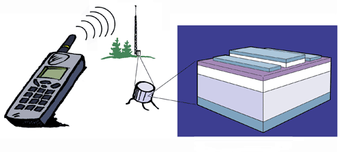
The first worked-out proposal for a heterostructure transistor was published in 1957 by Herbert Kroemer, then working at RCA (Radio Corporation of America) in Princeton, USA. His theoretical work showed that a heterotransistor can be superior to a conventional transistor, particularly for current amplification and high-frequency applications. A frequency as high as 600 GHz has been measured in a heterotransistor, i.e. about 100 times higher than the best ordinary transistors. In addition, the noise is low in amplifiers based on these components.

High resolution image (JPEG, 247 kB)
Fig. 1: In the fast transistors of the base stations of cell phones there are semiconductor heterostructures.
The heterostructure laser
Heterostructures have been crucially important for the development of semiconductor lasers. Zhores I. Alferov of the Ioffe Institute of the Russian Academy of Sciences in what was then Leningrad and Herbert Kroemer then at Varian in Palo Alto proposed in 1963, independently of each other, the principle for the heterostructure laser, an invention that is probably as significant as that of the heterotransistor.
Alferov was the first to succeed in producing a lattice-adapted heterostructure (AlGaAs/GaAs, 1969) with clear borders between the layers. Alferov’s research team succeeded in rapidly developing many types of components built up of heterostructures, including the injection laser which Alferov patented in 1963. A technological breakthrough occurred around 1970 when heterostructure lasers became able to work continuously at room temperatures. These properties have, for example, made fibre-optic communications practically possible.
 |
| High resolution image (JPEG, 243 kB) |
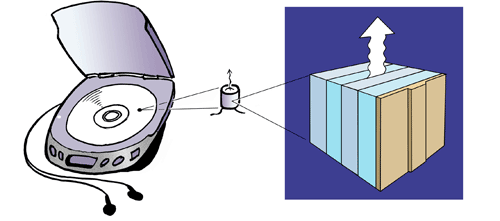
| Fig.2: The laser diode of the CD player contains a semiconductor heterostructure. |
The integrated circuit – the chip
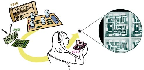
The invention of the transistor just before Christmas 1947 is usually taken to mark the start of the development of modern semiconductor technology (Nobel Prize in Physics 1956 to William B. Shockley, John Bardeen and Walter H. Brattain). With the transistor there came a component that was considerably smaller, more reliable and less energy-consuming than the radio valve, which thus lost its importance. The increasing complexity of a system using more and more radio valves meant that a practical limit had been reached with around a thousand valves. By soldering individual transistors together on a printed-circuit board the system could be increased to over ten thousand transistors.
Even though the transistor permitted an increase in the complexity of a system of individual components soldered together it soon became clear that the number of transistors was the limiting factor in meeting the needs of the emerging computer industry. As early as the beginning of the 1950s there were ideas and thoughts about manufacturing transistors, resistors and condensers in a composite semiconductor block, an integrated circuit.

High resolution image (JPEG, 476 kB)
Fig 3: Development has gone from radio valves via transistors to integrated circuits, chips, now in all modern electronics.
The people who were to demonstrate the practical possibility of an integrated circuit were two young engineers, Jack S. Kilby and Robert Noyce, working independently of each other. Kilby, however, was first with his patent application and Noyce knew of this work when he filed his own application.
The integrated circuit is more of a technical invention than a discovery in physics. However it is evident that it embraces many physical issues. One example is the question of how aluminium and gold, which are part of an integrated circuit, differ regarding their adhesion to silicon. Another question is how to produce dense layers that are only a few atoms thick.
It is thus obvious that the development of the integrated circuit prompted enormous investment in research and development in solid-state physics. This has not only led to development in semiconductor technology but also to gigantic development of apparatus and instruments. Continual miniaturisation, moreover, has come up against a number of material-physical limitations and problems that have had to be solved.
The notion of an integrated circuit was there. But ten years were to pass from the invention of the transistor before the technology involved had matured sufficiently to allow the various elements to be fabricated in one and the same basic material and in one piece. The invention is one in a series of many that have made possible the great development of information technology. The integrated circuit is still, after 40 years, in a dynamic phase of development with no sign of flagging.
Jack S. Kilby and Robert Noyce are both considered as the inventors of the integrated circuit. Kilby was the one who built the first circuit. Noyce developed the circuit as it was later to be manufactured in practice with silicon and silicon dioxide as semiconductor and insulator and with aluminium as the electrically conductive element. Both have on a number of occasions received prizes and distinctions.
Robert Noyce died in 1990. He was then honoured as one of the most important founders of Silicon Valley and for the leading role his company had played in the development of information technology, with the integrated circuit as a cornerstone.
Jack S. Kilby has continued his career as an inventor, with some 60 patents. Among other things, he is co-inventor of the pocket calculator, one of the first applications of the integrated circuit. A market survey run before the start of planning for its manufacture showed that interest in a pocket calculator was negligible. After all, people had slide-rules!
The Prize amount: SEK 9 million. Zh.I. Alferov and H. Kroemer are to share one half and J.S. Kilby is awarded the other half.
| Further Reading |
| Physics and the Information Revolution by J. Birnbaum and R.S. Williams, Physics Today, January 2000, p. 38. |
| Crystal Fire by Michael Riordan and Lillian Hoddeson, W.W. Norton & Company, New York and London 1997 (particularly Ch. 12). |
| Quantum Technology by Gerard Milburn, Allen & Unwin 1996 (particularly Ch. 4). |
| The History and Future of Semiconductor Heterostructures from the Point of View of a Russian Scientist by Zh. I. Alferov, Physica Scripta, vol. T68, p. 32, 1996. |
| Band Offsets and Chemical Bonding: The Basis for Heterostructure Applications by H. Kroemer, Physica Scripta, vol. T68, p. 10, 1996. |
| Materials for Information and Communication by J.S. Mayo, Scientific American, October 1986, p. 50. |
| Electronic and Magnetic Materials by P. Chaudhari, Scientific American, October 1986, p. 114. |
| The Chip. T.R. Reid, Simon & Shuster, New York 1984. |
| The genesis of the integrated circuit by M.F. Wolff, IEEE Spectrum, vol. 13, no. 8, August 1976, p. 45. |
| Invention of the Integrated Circuit by J.S. Kilby, IEEE Transactions on Electron Devices, vol. ED-23, no. 7, July 1976, p. 648. |
| Advanced information on the Nobel Prize in Physics 2000, The Royal Swedish Academy of Sciences (pdf). |
Zhores I. Alferov born 1930 in Vitebsk, White Russia, then the Soviet Union. Doctor’s degree in physics and mathematics 1970 at A.F. Ioffe Physico-Technical Institute in St. Petersburg (then Leningrad), Russia. Director of this Institute since 1987.
Professor Zhores I. Alferov
A.F. Ioffe Physico-Technical Institute
26 Politechnicheskaya st.
St. Petersburg 194021
Russia
Herbert Kroemer born 1928 in Germany. Doctor’s degree in physics 1952 at University of Göttingen. Employed at, among other places, RCA Laboratories, Princeton, NJ, USA 1954-57 and at Varian Associates, Palo Alto, CA, USA, 1959-66. Professor of Physics, University of Colorado, Boulder, 1968-76 and subsequently University of California at Santa Barbara, USA.
Professor Herbert Kroemer
Electrical and Computer Engineering Dept.
Room 4107 Engineering I
University of California
Santa Barbara, CA 93106-9560
USA
Jack S. Kilby born 1923 at Jefferson City, Missouri, USA. Employed at Texas Instruments since 1958. Professor at Texas A&M University 1978-85.
Dr Jack S. Kilby
Texas Instruments Incorporated
12500 TI Boulevard
Dallas, TX 75243-4136
USA
Nobel Prizes and laureates
Six prizes were awarded for achievements that have conferred the greatest benefit to humankind. The 14 laureates' work and discoveries range from quantum tunnelling to promoting democratic rights.
See them all presented here.
